10+ sdram block diagram
Functional Block Diagram 128 Meg x 4 x 16 Banks x 2 Ranks Figure 2. Cortex-A9 MPU Subsystem Block Diagram and System Integration 103.

Is42s16400j 7tl Memory Cad Models Datasheet Features Video Faq
Logic Diagram of a Typical SRAM CS 150 - Spring 2004 Lec 9.

. Pin Assignments 288-Pin DDR4 UDIMM Front 288-Pin DDR4 UDIMM Back Pin Symbol Pin. Memory Controller - 6 Typical SRAM Timing Write Timing. It is internally configured as an 8-bank DRAM Functional Block Diagram.
ACP ID Mapper 105. TwinDie 12V DDR4 SDRAM MT40A2G16 128 Meg x 16 x 16 Banks x 1 Ranks Description The 32Gb TwinDie DDR4 SDRAM uses Microns 16Gb DDR4 SDRAM die. 1Gb DDR2 Part Numbers Package Pb-free 84-ball 8mm x 125mm FBGA 60-ball 8mm x 115mm FBGA 60-ball 8mm x 100mm FBGA Lead solder 84-ball 8mm x 125mm FBGA.
See Functional Block Diagram for pins specific to this module. SDRAM Controller Subsystem Block Diagram 63. Two x8s combined to.
It consists of three modules. WE_L A W rite Hold Time W rite Setup Time A OE_L. To estimate the power consumption of DDR4 SDRAM it is necessary to understand the basic functionality of the device see the following figure.
LPDDR3 Block Diagram 64GBs. Features of the SDRAM Controller Subsystem 62. The functional block diagram of the SDRAM controller is shown in Figure 2.
SDRAM 100-200 x4 x8 x16 x32 400 MBs 100-200Mbs 64Mb - 512Mb 66ns 1W DDR1 100-200 x4 x8 x16 800 MBs 200-400Mbs 128Mb-1Gb 60ns 1W. X4 x8 TwinDie DDR4 SDRAM Functional Block Diagrams Functional Block Diagrams Figure 1. SDRAM Controller Subsystem Interfaces.
Features of the Cortex-A9 MPU Subsystem 102. Functional Block Diagram 256 Meg x8 DDR3 SDRAM is a high-speed CMOS dynamic random access memory. X4 x8 x16 DDR SDRAM Functional Block Diagrams Functional Block Diagrams The 1Gb DDR SDRAM is a high-speed CMOS dynamic random access memory containing 1073741824.
SDRAM Controller Memory Options 64. For DDR4 UDIMM modules. The operation of a DDR4 de-vice is similar.
The main control module the signal generation module and the data path module.
2
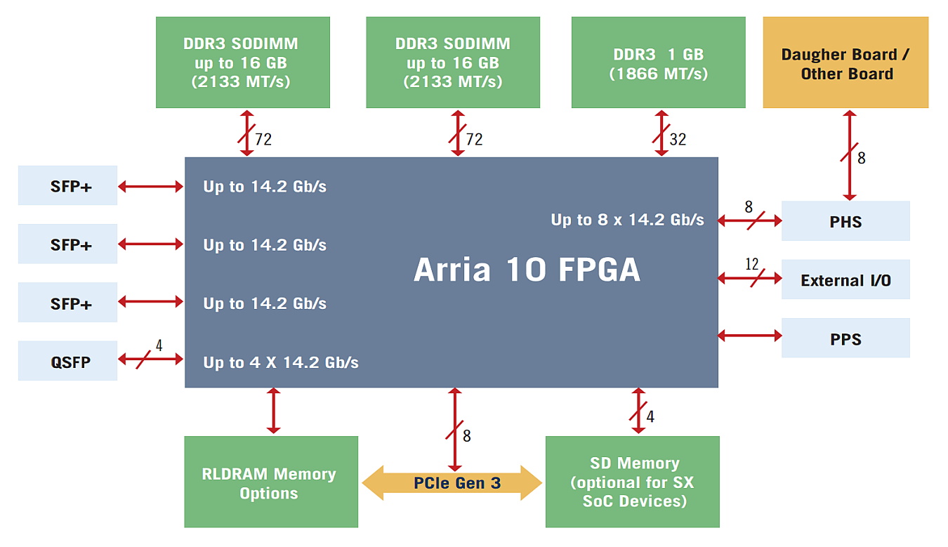
Gidel Proc10a Fpga Accelerator Board With Intel Arria 10 Gx Sx Sky Blue Microsystems Gmbh
2

Gidel

Row Hammer Wikiwand
Live Practical Class Of How To Identify Primary And Secondary Voltage Youtube

Rgb Video Out Block Diagram Video Logic

Memory Cell Computing Wikiwand
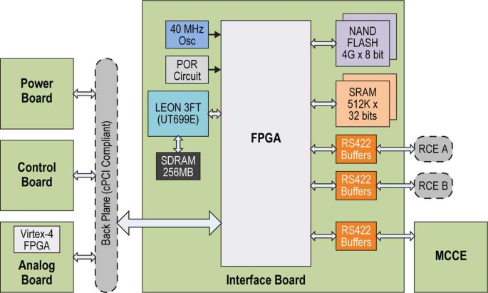
Tacsat 4

Stm32f429zit6 Microcontroller Datasheet Reference Manual Pinout Faq
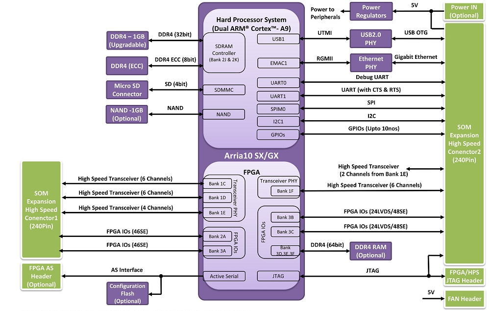
Intel Arria 10 Soc System On Modules Iwave Systems Mouser
Pixl Planetary Instrument For X Ray Lithochemistry Springerlink

Delay Line Memory Wikiwand
Introduction Springerlink
2

Memory Cell Computing Wikiwand
How To Design A 4kx8 Bit Memory System By Using 1kx4 Bit Memory Chips Quora